DARPA-backed Startup Speeds Up Production for Radar, Electronic Warfare Amplifiers
New method cuts production time for traveling-wave tubes from over a year to weeks, supporting radar and electronic warfare systems.
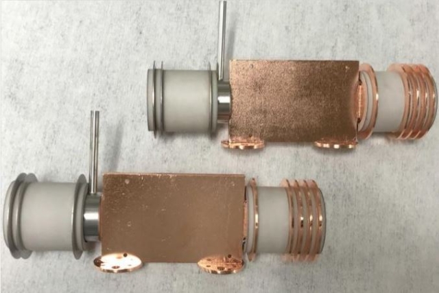
A U.S. startup, supported by the Defense Advanced Research Projects Agency (DARPA), has developed a new manufacturing process that reduces the production time for traveling-wave tubes (TWTs) from over a year to just a few weeks.
TWTs are used in high-frequency applications, including satellites, deep space communication, and electronic warfare. Their complex design and precise assembly require specialized manufacturing, which has traditionally limited supply and increased costs.
Elve, a deep-tech startup, developed the Layered Additive Multi-Material Manufacturing – Digitized (LAM3D) process through DARPA’s Small Business Innovation Research (SBIR) program. This new additive manufacturing technique enables faster production and reduces costs, making TWTs more accessible for both defense and commercial use.
The LAM3D process also allows Elve to design and optimize TWT circuits in under two hours across critical frequency bands such as Q-band (33–50 GHz), V-band (40–75 GHz), and E-band (60–90 GHz). These frequencies are essential for advanced radar systems and high-speed communication networks.
Elve’s innovation received additional support from DARPA’s Embedded Entrepreneur Initiative (EEI), which connects startups with business experts to accelerate commercialization. Through EEI, Elve refined its market strategy and raised $15 million in Series A funding to open a commercial manufacturing facility.
Building on its DARPA-supported work, Elve has expanded the LAM3D process to manufacture circuits operating above 200 GHz, meeting future demands for next-generation communication and sensing technologies.

U.S. Navy, DARPA Develop Robotic System for Satellite Servicing

Raytheon Secures DARPA Contract to Develop Next-Generation Ultra-Wide Bandgap Semiconductors

Aurora Flight Sciences Advances Real-Time Adaptive Control for Uncrewed Surface Vessels in...
Lockheed Martin Wins $4.6M DARPA Contract for AI-Driven Airborne Mission Tools
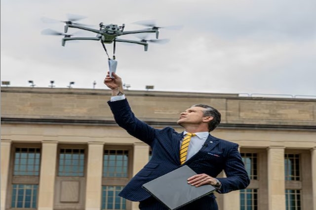
Pentagon to Arm Warfighters with ‘Made in America’ Low-Cost Drones
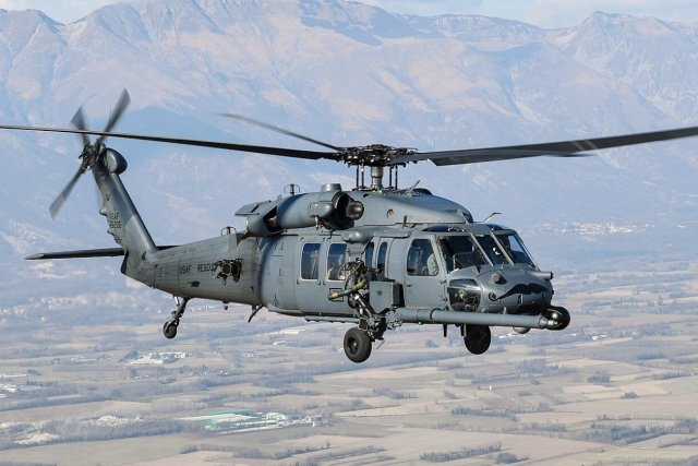
Norway to Buy 9 Sikorsky HH-60W Helicopters Worth $2.6 Billion
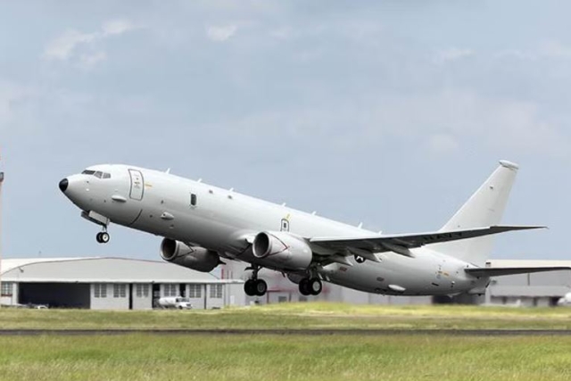
L3Harris Delivers First Overhauled P-8A Poseidon from 139-Aircraft Navy Fleet

South Korea’s DAPA Finishes Incheon Class Frigate Search Radar Upgrade

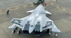
China's Mass-produced J-35A Aircraft Set to Disrupt Global Stealth Fighter Market
China is aiming to disrupt the global stealth fighter market by mass-producing its fifth-generation J-35A at a pace comparable to...

The Future of Combat: Miniaturized Laser Weapons Set to Replace Bullets and Missiles
Lasers may soon replace bullets, and drones could disable enemy UAVs with beams of light instead of missiles

Four-legged Robots Vs. Military Dogs
Four legged robots that resemble dogs are increasingly being seen in war zones and exercises for functions such as reconnaissance...

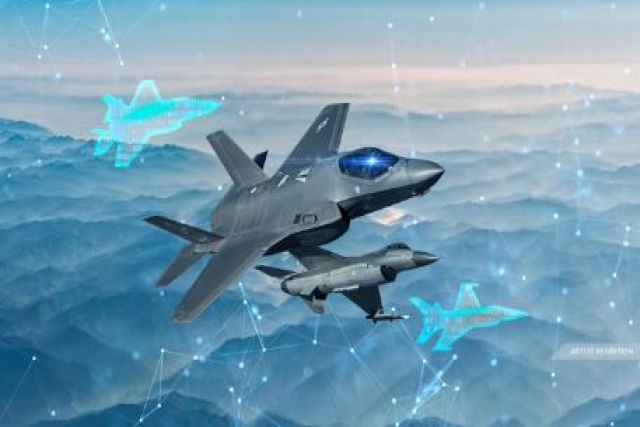
Lockheed Martin Faces Billions in F-35 Cuts Under U.S. Policy Shift
Americas policy of controlling F-35 usage, spares, and maintenance—combined with President Donald Trumps threats of trade wars with Europe, halted...
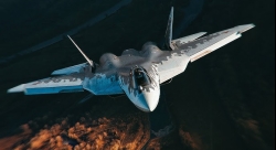
Russian Su-57 and Chinese J-20 as Alternatives to the American F-35 Stealth Fighter
As the Russian Su-57 stealth fighter jet enters serial production, the debate over how it stacks up against the American...